Micro Projects Home Page

Home

 8085 Project Page

WELCOME TO MY 8085 PROJECTS PAGE!!

As there are so many Universities and Colleges out there Worldwide that are still using this particular micro as an example of a typical 8 bit processor, this page is therefore dedicated to you folks, and hopefully it will guide you in the right direction.

 Microprocessor Basics

Micro Basics

Site Projects

Site Projects

Construction Techniques

Construction

Programming concepts

Software

Projects

Projects

So what sort of project do I have in mind then? Well, as the actual design will vary - depending on what YOU have in mind, I have gone for a middle-of-the-road approach with my circuit, choosing an idea that can easily be extended or altered. Thus the basic 8085 processor module (with 295 byte bare-bones software package) does the elementary, though interesting task of identifying the HEX representation of a character sent out the comms. port of a computer / terminal / PC or Mac. In order to do this, the board uses a total of 10 chips, plus a quad HEX display with built in driver. 

I.C PARTS LISTING

8530 SCC

Zilog 8530 SCC

8085 Processor

I  used a Mitsubishi M5L8085AP device

Z8530 SCC

Universal dual UART from Zilog - I used a spare Z0853006PSC

28C64 / 2764

EEPROM or EPROM for completed project. 8K x 8 bit device

6116 RAM

2K x 8 bit static RAM. Easily expandable. I used an HM6116P-3 but you can use something bigger.Simply add the extra address lines..

74LS273

HC should work fine too. Octal latch for multiplexed A/D bus

7414

HC/LS should work fine too. HEX inverting schmitt triggers

74LS139

Dual decoder. One half for memory, other half for the I/O selection

74LS244

Optional octal tristate device for switch inport. Not used in my CCT

74LS00

Again, HC should work fine here. Quad NAND gates

MAX232CPE

THE industry standard RS232 driver chip. Single +5V supply rail too!. Only use if RS232 required RS422 etc. needs different chip. See my section on the Prom Programmer for the MAX232 circuit.

8085 page

8085 page

Fault Finding

Fault Finding

Data Sheets

Data Sheets

EEprom Programmer

Programmer

MISC. PARTS

8085 board from front

8085 board front view

2.4576MHz xtal

VERY important frequency as it indirectly supplies Baud Rate clock

DL1414 display

One of my favourites. Swap for whatever you like using, though the software may need small changes to accommodate it

Reset button

Single pole - any sort

47u 16 Volt cap

For reset circuitry

100nF caps

A dozen or so scattered around the board for decoupling purposes

10u 16V cap

Minimum of one for board decoupling again

1N4148 diode

Part of reset circuitry

IC sockets

2x40 pin, 2x28 pin, 1x24 pin, 2x20 pin, 2x14 pin, 2x 16pin

Misc. caps

Four or five caps. will be needed for the MAX232 circuit if used

Project board

Use Vero / strip board or your favourite prototype pad board etc.

Video Information

VIDEO info

Peripheral Circuitry

Peripheral circuitry

Central Heating and Z280's

Z280 and  Central Heating  Controllers

Concluding Ideas

Concluding ideas

Links

Links

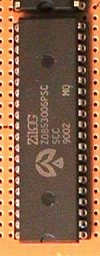
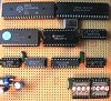
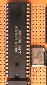
THE CIRCUIT

Nothing special here, but note that I�ve only used the single octal latch to interface to the 8085�s multiplexed bus. Some people use up to three for this, but I�m making it simple but perfectly reliable by using only one! This is  used to buffer the lower order 7x address lines. The 8085 needs no external oscillator unlike some processors (hooray!). As we are economising on hardware here, we�re using the clock output of the CPU to provide the SCC with it�s Baud Rate drive, hence the frequency MUST be 2.4576MHz.(or it just won�t communicate properly) The DL1414 alpha-numeric display I�ve used interfaces directly to the 139 decoder. I�ve actually used 2 of these on my prototype to give 8 digits in total. The software however only needs to see the LOWER ORDER one to display the results of the HEX comms test. (for those of you not wishing to fork out for two) It�s likewise a relatively straightforward task to interface and decode the output to 2x standard 7 segment LED displays to show the lowest 2x digits containing the HEX decoded information. I have included a 74LS244 tri-state buffer chip for anyone wishing to add any extra switches to the project. This is already wired to be accessed via the I/O 74LS139 decoder at address 30H.

8085

8085 and 2.45M crystal

SOFTWARE NOTES

A very important observation to note here. If altering or adding to the programming info given here, do ensure that you ONLY use those programming steps that are meant for the 8080 or 8085. NONE of the Z80 steps will work and will throw you completely off-course if you do. Half the problem is that 8080 / 8085 programming steps don�t include certain basic items such as relative jumps! OK own up Izabella, WHO inadvertently used a couple of Z80 steps when writing software for their latest 8085 project?   :)

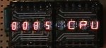
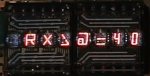
RESET

Note that after a hard reset, the project sets up the display to read:: �8085 CPU�. Of course, if the lower order one is fitted on it�s own, this will simply bring up: �CPU�. As soon as the first byte is received by the SCC, the display will change to: � RX>x=xx� with the x�s replaced by the ASCII (if displayable by the display, or blank if it can�t), plus the two HEX digits to the far right - i.e. in the display address locations 00H and 01H. A single ASCII 07H, �BELL� is sent at Reset..

STACK

Entends downwards from the top of the RAM. In the case of my prog. this is at 4800H

DISPLAYS

LSD is 00H, 01H, 02H and 03H. If using the second display these are from 10H - 13H

RAM

From 4000H to 47FFH. A total of 4 memory segments are decoded by the 139 i.e. 16K each. This is the single device limit that may be used without altering the decode circuitry.

ROM

The given circuit permits either an 8K EEPROM or 8K EPROM to be used.

INPORT

Available but not used by my software. Accessed by an I/O read to address 30H

SCC

Both read and write registers are accessed with I/O addresses 2x

INTERRUPTS

None used with all hard-wired low.

SID and SOD

Eh? You�ll know what I�m on about! CPU on-chip serial I/O of course - not used here

COMMS

Is set up for 2400 baud, 8 bits, 1 stop bit, no parity

I at = +5 Volts

405mA after RESET with 2x DL1414 displays, 375mA with just the RH (LSD) display. I calculated that by using a CMOS 80C85 and 74HC chips, these figures will be a lot lower. Thus one can logically deduce that my figures are the maximum the cct will take.

VARIOUS SUBROUTINES FOR YOUR POSSIBLE USE?

SEND BLOCK OF 4x CHARS TO RH DISP.

Put 4x chars. in memory, then point the HL pair to them (21xxH)and GOSUB 0058H

SEND BLOCK OF 4x CHARS TO LH DISP.

Put 4x chars. in memory, then point the HL pair to them (21xxH)and GOSUB 0048H

TRANSMIT ONE CHARACTER

Put single character in location 4000H then GOSUB 0083H    (CD,83,00H)

WAIT IN LOOP TO RECEIVE A CHAR.

GOSUB 00B4H then when prog. exits loop collect character from address 4001H

Useful 1mS DELAY

Very approx. delay value GOSUB 007CH

8085 board wiring side

The 8085 project from the back of the board

reset display
information display

To the left we see the display seen immediately after a hardware reset.


The lower one shows the screen after the first data word arrives. In this case it was an �@� which is an ASCII HEX code of 40

The three links opposite should give all the information needed to successfully build the project. I used the core wiring list myself to construct the prototype so there shouldn�t be any errors in it. Likewise, the complete program listing was downloaded from the working prototype�s own EEPROM (from my example of the site�s �Prom Programmer� so the chances of any errors here are also pretty unlikely.

http://www.hampshire-shops.co.uk

8085 Program listing
8085 core wiring
8085 schematic

Click on the icon to the left for the full 8085 project program listing as used with the prototype..

Click to the left for the �Core� wiring list I used to construct the protype. This contains all the main busses and power wiring .

This icon is for the schematic diagram for the 8085 project. By nature it is quite large so please be patient!