Microprocessor Basics
Micro Projects Home Page

Hi all! Having seen the same simplified �how a microprocessor works� in so many publications - I would like to put forward my own simple analogy that may prove to be better understood. OK. So first and foremost let us think of the micro as being a very obedient person - who, intellegent as they might conceivably be, will follow the instructions on his list whatever the end result. To expand upon this a little more, it must be pointed out that each and every instruction involves essentially ONE action.

Home

 Microprocessor Basics

Micro Basics

Site Projects

Site Projects

Construction Techniques

Construction

Programming concepts

Software

Projects

Projects

8085 page

8085 page

Fault Finding

Fault Finding

Data Sheets

Data Sheets

EEprom Programmer

Programmer

Video Information

VIDEO info

Peripheral Circuitry

Peripheral circuitry

Central Heating and Z280's

Z280 and  Central Heating  Controllers

Concluding Ideas

Concluding ideas

Links

Links

Picture

Take as a simple idea, that of picking up a message from a post box and transferring the message content to another. Whilst this sounds an easy task, it is ideally suited for our programming example as it can be used to identify several essential microprocessor �states�.

1

Pick up the list of instructions.

In programming, this is the hardware RESET. The micro turns to page ONE (the starting address) in the READ ONLY MEMORY (ROM)

2

Instruction one says go to the letter box with the 6 on it, make a perfect COPY of what�s inside and put it in your pocket.

In a program this would be an I/O (input / output) command. Go and READ in a value from a specific  ADDRESS and place it in a REGISTER

3

Instruction two says put a COPY of what is in your pocket into the letter box with the 9 on it

Another I/O instruction. But this time it tells the micro to COPY what it happens to have in it�s register into a different ADDRESS

4

Instruction three says stand still and stop reading the instructions!

This is the equivalent of a HALT instruction. Not one of the more commonly used ones, but there to be obeyed all the same.

More Detail? OK

The HARDWARE RESET is usually actioned by taking one of the processors pins either high or low for a minimum number of clock cycles. Once the line is restored to it�s previous level, all of the programming registers will be cleared, counters restored etc. and the program counter (the page �one� in the book, set to the first address.

The first instruction - the I/O read will generally be two bytes long minimum. One to tell the processor to DO the instruction, and the second being where to DO it - i.e. the address. The HARDWARE MUST be electrically configured such that the processor will FIND the value at that specific address.

The second instruction says put what�s in the register into a second I/O address - once again to be set up in HARDWARE where the processor expects it to be. If it is NOT set up correctly, the processor will still send it out, but it will of course disappear into the ether.

In my humble experience, it is the I/O instructions that cause the most confusion to the novice. We can all play around with those register instructions, adding this to that, storing this here, EXORing that over there. NEVER will the programming manual actually tell you HOW that value ended up in the register  in the first place! Equally mystifying can be just how one LOOKS at the final result! The trouble with doing a spot of assembler/machine code with a computer like a PC is that one never needs to know; it just comes in from the keyboard and magically appears on the screen! It is this reason that I will dwell a little longer on the I/O subject than that of the memory as I feel that this is the �bit� that most needs to be understood.

Picture

Let�s quickly compare the two port ideas then. The more complex with it�s decoder chip, is using two ADDRESS lines from the micro to decode the correct address. The R/W line is then applied to the CLOCK line of the decoder. A NEGATIVE EDGE signal will probably be needed here. Note that the processor READ / WRITE line only enables the decoder during a processor WRITE - hence this is a simple OUTPORT circuit.

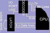
Both the I and the O parts are accessed by the micro in an almost identical manner. With some processors, the I/O is addressed by the same decoder as  the memory - i.e. all DATA TRANSFERS take place at specifically chosen addresses. With some other families, special I/O pins are available from the micro to select the I/O devices with a modified access cycle .

Picture
Picture

So the above diagram looks as if it has been oversimplified perhaps? Well it hasn�t! This is just how a large number of micro�s access their I/O. Now if you really want to see a simple example, try the example to the left; almost as simple as it possibly can be - yet it too works!

In the second simpler example, as this is a barebones method with few hardware RESOURCES, we can use the unused address line A15 without the decoder. Note though that the hardware will require a NEGATIVE signal as before, so as the ADDRESS lines are generally POSITIVE going, we need to wire in an INVERTER gate before applying the address signal to the buffer�s  Chip Enable. If an OCTAL BUFFER chip is used here, we have a simple INPORT circuit.

Picture

A quick word about TRISTATE for those who may be unsure of it�s meaning. Without the ability to TRISTATE bus devices, microprocessor�s as we know them could not exist. If you remember that the processor�s DATA BUS lines will be connected to (at the very least), three or more devices at once, by making these devices tristate, we allow any OUTPUTS on the bus to go high-impedance - i.e. their customary output voltages are not permitted to interfere with the activity on the bus that does not concern them. Using the tristate enable lines, we are able to physically SELECT the HARDWARE of our choice onto the bus only when it is called for.

Another important example of when �tri-state� lines are used is where the micro has it�s DATA and ADDRESS lines �multiplexed�. This is usually done when there are insufficient pins on the package for separate busses. With these chips you will find some sort of ADDRESS/DATA switching line that tells the HARDWARE whether it�s address or data information on the bus at any one time. This line will usually be connected to some form of hardware LATCH device that will be able to �latch� in the address data, so when the data data follows along afterwards, it will be routed to the correct destination.

Once again I think it important to point out that the above examples will only apply to SOME processors. The example using the �spare� address line A15, will not work if the processor is one that resets to the TOP of the memory, such as the 6502, the 6800 or the 6809. It WILL however work with the Intel  8088 / 8086 / 186 / 286 series (which also looks for reset information high up in the memory) because they have additional address lines above A15, one of which may be used for the same ends.

Picture

INTERFACING I/O DEVICES

I/O devices are accessed in much the same way as the memory, though they sometimes need addressing by an external addressing device or decoder. The most basic devices being simply latches or even buffers, enabled by a decoder or I/O line. In the case of the TIL311 display device  shown above, the package incorporates not only the LED segments, but also the binary to segment decoder AND a data latch! You can see the actual chip itself in the bottom half of the device. All in all, a very easy and convenient display to use, as all one does is connect it�s four data lines straight up to the processors data bus, and the strobe to the I/O decoder. Voila! Note that it only has four data lines, so you have to decide whether to connect to the top half of the bus or the lower half. Of course if using two TIL311�s, one could use the LOWER four bits for one display and the UPPER four bits for the other. By commoning the enable lines, one could then update them in the program simultaneously from the same byte! (assuming an 8 bit processor)

Although PIO and PIA multi I/O LSI chips offer many different interfacing options, as a general rule, I tend to avoid them unless these facilities (such as interrupts) are really needed, as it is usually simpler to use either two or three tri-state latches or buffers. The ones I most commonly use are the 74xx373 or 374 octal latches, or the 74xx240 241 244 series octal buffers. Where bi-directional tri-state buffers are needed - such as that required with a multiplexed data / address bus, I generally opt for the 74xx245. Where space is at a premium and if only 4 bits are needed, the 74xx125 is a viable alternative tri-state device in a 14 pin pack. (The others all mentioned above are 20 pin.)


Picture

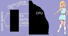
INTERFACING MEMORY DEVICES

Memory is something that all micro�s need to interface to. It will be noticed that there is almost a �standard� for the pin layout used by most of these - which can be very useful at times. Have a look at a few of the pinouts in the Data Sheets section to see for yourself.

Memory is connected by it�s ADDRESS and DATA lines to the processor and accessed via it�s chip select and memory read / write lines. This is where the chips vary a little with capacities and type. Almost ALL will be accessed by taking their enable lines LOW. Read / Write lines invariably need the line taken low to WRITE.

A memory device may have more select lines than you need - i.e. /CE1 (chip enable 1) /CE2 (chip enable 2) and /OE (output enable) etc. You only have to use those that you need. Simply hard-wire-enable the ones that you don�t need, remembering that an output enable (for example) can�t enable anything if the chip itself is not enabled with the /CE lines.

Picture

TO BUFFER OR NOT TO BUFFER?

Although it is necessary to buffer data and address lines if the number of devices on the bus exceeeds the drive capability of the microprocessor, I�ve never found this necessary with any of my home micro projects.

Of course there is nothing exactly difficult in inserting buffering devices in the bus, (as long as one remembers to add in their propogation delay when calculating timing values), it�s really just the extra drag of wiring the things in! The best way to ensure that your circuits won�t need them is to use HC (high speed CMOS) devices wherever possible.

LOGIC FAMILIES

A quick word to conclude this page is the question of logic families. Further to my comment above about bus drivers, out of choice I always go for the 74HC series of IC�s. The HCT family was created to give TTL �compatibility� but as a rule I don�t use it as it has a greater susceptability to noise. Assuming that all devices are working within spec. and no busses are overloaded then there is no reason whatsoever why TTL  standard/LS/HC/HCT and even 4000 series CMOS should not work reliably together. I can say in all honesty that I�ve never experienced a problem with any combination in a home micro project.

http://www.hampshire-shops.co.uk